
Challenges of a Schematic Designer
Every schematic designer faces some key challenges. This blog highlights those challenges and suggests some ways to work around them.
PCB DESIGNELECTRONIC SYSTEM DESIGNSCHEMATIC ENTRYLIBRARY MANAGEMENT
Atanu
8/2/20263 min read

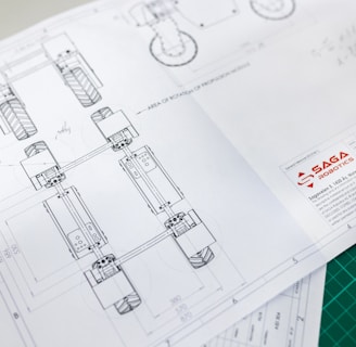
Schematic design, PCB layout, and high-speed engineers face a distinct but overlapping set of technical challenges that span component selection, signal integrity, power integrity, EMI/EMC compliance, thermal management, and design for manufacturability (DFM). These challenges have intensified with the proliferation of high-frequency designs (>1 GHz), advanced protocols (PCIe Gen 5/6, USB4, DDR5, PAM-4), and miniaturization trends (HDI,chiplets, heterogeneous integration).
Schematic design engineers are responsible for capturing the logical design of a circuit, selecting components, defining net connectivity, and ensuring the design is electrically sound before layout begins.
Component Selection and Library Management: Poorly managed or decentralized component libraries are major bottleneck in PCB Design, often causing more delays than schematic or layout work. This is often overlooked by companies that have small design teams. Each team works with an expected level of autonomy for component selection. This leads to some key issues:
Incorrect outdated component footprints: Mismatched footprints cause issues during PCB layout and assembly, leading to respins.
Missing or incorrect manufacturer part numbers (MPNs): Many components have multiple variants, and all variants need correct MPNs for searchability and procurement.
Lack of datasheet access: Designers need immediate access to datasheets alongside component models to verify electrical and mechanical specifications.
Redundant component models: Decentralized libraries lead to duplicate or inconsistent component data, causing confusion and errors.
Non-compliant footprints: Component footprints that do not obey IPC-7351 or manufacturer specifications can lead to assembly failures.
To mitigate some of the above challenges we recommend:
Using Centralized Component Libraries: The whole design team using a central repository with data sharing and visibility for all team members. It becomes even more important when upgrading an older design design to the newer version - carefully updating all components and footprints to the latest version.
Automated library management tools: Leverage ECAD software with API access to distributor databases real-time databases for real-time sourcing data updates.
Standardized symbols, footprints and 3D model: Ensure all components three pieces of data for effective electrical and mechanical integration.
As an example Cadence Design Systems products like Capture allow the user to access external parts. For more details see here.
Challenge #1: Schematics errors that pass unnoticed can lead to costly respins and field failures.
Key Issues:
Missing or incorrect power and ground connections: Can lead to circuit malfunction or complete failure.
Improper or missing net labels: Causes confusion during schematic-to-PCB conversion and increases debugging time.
Ignoring ERC warnings: Hidden connectivity or logic issues may remain undetected until prototyping.
Inconsistent reference designators: Makes debugging and manufacturing difficult.
Overcrowded or poorly organized schematics: Reduces readability and increases the chance of design errors.
Using incorrect component values or outdated datasheet information: Can result in electrical mismatches or reliability issues.
Recommendations:
Rigorous ERC enforcement: Treat ERC warnings as errors and resolve them before proceeding to layout.
Schematic review checklists: Implement peer reviews with standardized checklists for power, ground, net labels, and reference designators.
Version control and change management: Use PLM (Product Lifecycle Management) tools to track schematic revisions and component changes.
Challenge #2: Inadequate power distribution planning at the schematic stage can lead to power integrity (PI ) issues that are difficult to fix in layout.
Key issues:
Insufficient decoupling capacitor planning: Missing or improperly sized decoupling capacitors near IC power pins can lead to voltage fluctuations and noise.
Incorrect power rail sizing: Narrow traces or undersized vias can cause IR drop and overheating.
Lack of bulk capacitance planning: Missing bulk capacitors for low-frequency ripple filtering can destabilize power rails.
Recommendations:
Decoupling strategy documentation: Specify decoupling capacitor values (e.g. , 0.1 µF, 10µF) and placement near power pins in the schematic.
Power tree diagrams: Create power distribution diagrams to visualize voltage domains, current requirements, and decoupling strategies.
Early PDN simulation: Use SP networks before layout.
In many cases the design team is hard pressed for time and/or resources to implement these detailed checks. You could outsource these validation and verification activities as that brings in a couple of advantages:
Brings in an outside perspective without bias and is easier to call out the issues.
Augments your resources with limited expenses.
We are just a phone call away to help with such services. Click here to get in touch.

